Case Study Resolving EMI in Medical PCB Circuit Diagram Mastering high-speed PCB routing techniques for EMI reduction is crucial in today's electronic design landscape. By implementing the strategies outlined in this guide - from optimizing layer stack-ups and differential pair routing to careful power distribution and post-layout mitigation techniques - designers can significantly reduce the
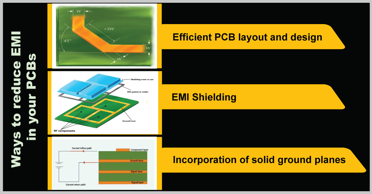
PCB Layout Techniques for Minimizing Crosstalk and EMI . Fortunately, a well-crafted PCB layout strategy can significantly reduce crosstalk and EMI. Here are some key techniques to consider: 1. The Power of the Ground Plane . The ground plane is an often overlooked yet essential element in PCB design.

Tips and PCB Design Guidelines for EMI & EMC Circuit Diagram
Discover PCB design practices for reducing EMI and improving EMC. Optimize your designs with component isolation, EMI filtering, and OrCAD X tools. Learn essential PCB design guidelines for EMI reduction, enhance EMC, and achieve reliable signal integrity. Explore strategies for components, layout, and OrCAD X. It is best to use separate
7 design guidelines for EMI and EMC reduction in a PCB. How do you design a board with low or absolutely zero electromagnetic interference? Well, it isn't impossible. The design practices below will make sure you do not create antennas that emit electromagnetic energy. These best design practices will reduce the length and area of the
Designing PCBs For EMI Management Circuit Diagram
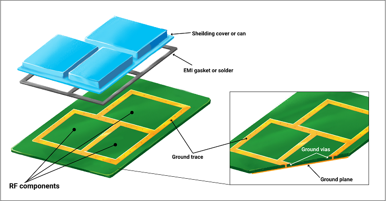
Shielding can be very effective, but it is never a good idea to rely on a shield to solve all EMI issues. This is very often not a viable solution and the best idea is always to use best practices for PCB design and layout, and use shielding as a backup or an additional layer of protection. 9. Impedance Control Mastering the art of PCB design for EMI reduction is paramount in ensuring the flawless operation of electronic devices and achieving EMC in a wide range of applications. A best practice in design is to place components that process similar types of signals in close proximity and separate them from components handling different signal types